

What if a diode’s published junction-to-ambient thermal resistance doesn’t predict its temperature on your board? Surface mount diode thermal resistance junction-to-ambient optimization starts by treating θJA as a test-condition result, not a fixed property of the component. The PCB, copper area, airflow, and enclosure all shape the heat path your design actually provides.
It’s reasonable to use the datasheet value as an early reference. But a calculated junction temperature can look safe while relying on assumptions that don’t match the finished assembly. To make a sound decision, identify the stated test conditions, estimate heat flow through your layout, and validate the result under representative operating conditions.
This article explains what θJA represents, which board-level and operating changes can improve heat transfer, and how to compare those changes systematically. You’ll also learn how to assess thermal margin on representative hardware and check the selected diode’s limits against its manufacturer datasheet. The goal is a defensible design decision based on the actual heat path, not an isolated number.
Key Takeaways
- Interpret θJA in the context of its stated test conditions; don’t treat it as a fixed value for every PCB or enclosure.
- Trace heat from the diode junction through its package and solder joints into the board to identify practical heat-flow paths.
- Compare loss reduction, copper spreading, vias, airflow, and package options based on design dependencies and a consistent validation method.
- Apply Surface mount diode thermal resistance junction-to-ambient optimization through a repeatable workflow that records the part, board revision, operating point, ambient conditions, and test setup.
- Translate validated thermal and electrical requirements into controlled BOM details, including package, ratings, quality requirements, and approved alternatives.
What Junction-to-Ambient Thermal Resistance Means for a Surface-Mount Diode
Junction-to-ambient thermal resistance, written as θJA, describes how much the diode’s semiconductor junction temperature rises above ambient for each unit of power dissipated. It is a thermal metric measured under specified conditions, not a stand-alone description of how hot a diode will run in every circuit. A datasheet θJA value describes performance under its stated test conditions; it does not guarantee the same result in your application.
For engineers evaluating Surface mount diode thermal resistance junction-to-ambient optimization, that distinction matters. θJA helps frame the thermal problem, but the board, enclosure, airflow, and operating point determine whether the test setup represents the product.
How θJA relates to junction temperature and power dissipation
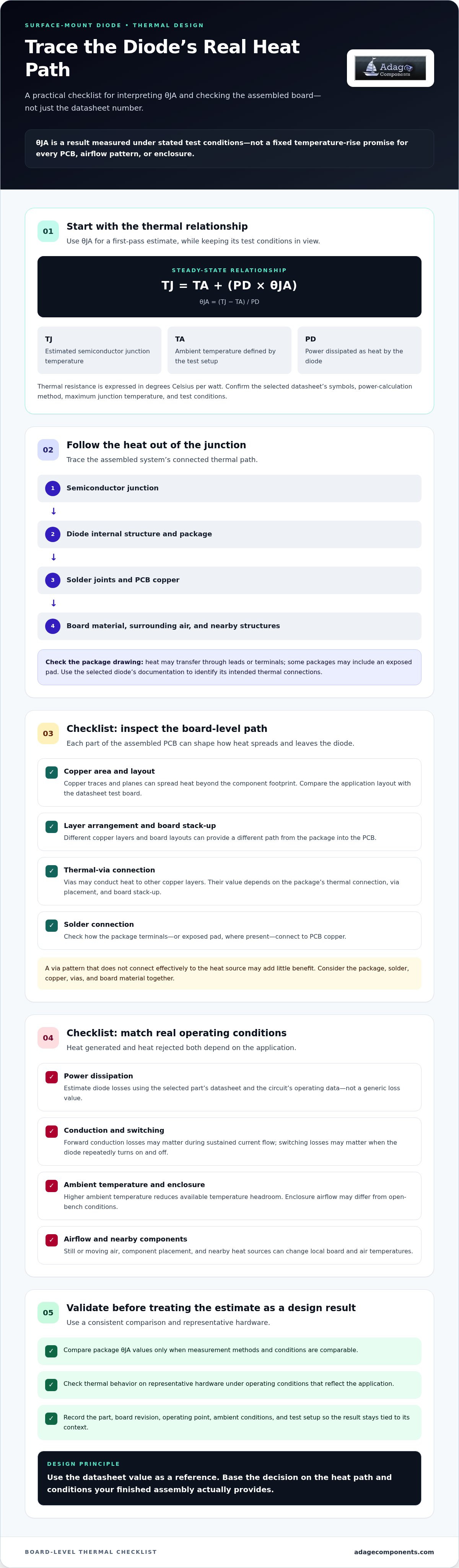
At steady state, the relationship is commonly expressed as θJA = (TJ − TA) / PD, or rearranged as TJ = TA + (PD × θJA). Here, TJ is the estimated temperature at the semiconductor junction, TA is the ambient temperature defined by the test setup, and PD is the power dissipated as heat by the diode. Thermal resistance is expressed in degrees Celsius per watt.
The equation shows that higher dissipated power or higher θJA produces a greater estimated junction-to-ambient temperature rise. It’s a useful first-pass calculation, but it assumes the stated conditions and steady state. Confirm the selected diode datasheet’s symbols, power calculation method, maximum junction temperature, and test conditions before using the result. The broader principles of thermal management to improve reliability help explain why controlling heat flow matters across electronic systems.
Why the datasheet number may not predict your PCB temperature
A datasheet θJA is tied to a particular setup. The test board’s copper area, layer arrangement, and layout can differ from the application PCB. Ambient temperature, still or moving air, component placement, and measurement method also affect the reported value. If the actual board has less effective copper spreading or sits in a warmer, enclosed space, its thermal path may differ substantially from the test arrangement.
Use θJA carefully when comparing diode packages. Values can support a package-level comparison when measurement methods and conditions are comparable. They’re less reliable as direct predictions of system-level temperature when test boards, environments, or operating conditions differ. Don’t treat one θJA number as universal across layouts and enclosures. For Surface mount diode thermal resistance junction-to-ambient optimization, use it as a reference, then assess the board-level design under representative conditions.
How Heat Travels from a Surface-Mount Diode Through the PCB
Heat starts at the semiconductor junction, where electrical losses occur. It moves through the diode’s internal structure and package, then across solder joints into the PCB. From there, heat spreads through copper and the surrounding board material before reaching the air and nearby structures. The PCB is part of the diode’s thermal system because its materials and layout shape the path from the junction to the environment.
The exact route depends on the package. Some packages transfer heat mainly through their leads or terminals; others may include an exposed pad. Use the selected diode’s datasheet and package drawing to identify the intended thermal connections rather than assuming a particular construction. A useful reference, Texas Instruments’ Evaluate Junction Temperature Properly, explains why thermal metrics must be interpreted in the context of the board and measurement conditions.
Package, solder, copper, and thermal-via contributions
Solder joints connect package terminals or an exposed pad, where present, to PCB copper. Copper traces and planes can spread heat beyond the component footprint, distributing it over a larger board area. Vias may conduct heat to other copper layers, but their value depends on the package’s thermal connection, via placement, and board stack-up. A via pattern that doesn’t connect effectively to the heat source may add little benefit.
These routes form a network, not a single path. Package construction, solder connection, copper geometry, vias, and board material all influence how heat spreads. That’s why Surface mount diode thermal resistance junction-to-ambient optimization must account for the assembled PCB, not just the component footprint.
Operating conditions that change the thermal result
Heat generation depends on how the diode operates. Forward conduction losses may be important during sustained current flow; switching losses may matter in circuits that repeatedly turn the diode on and off. Which sources dominate depends on the diode and its electrical operating conditions. Use the selected part’s datasheet and the circuit’s operating data to estimate dissipation, rather than applying a generic loss value.
Heat rejection also changes with conditions around the board. Higher ambient temperature reduces the temperature headroom available, nearby components can warm the local air or board, and enclosure airflow can differ from open-bench conditions.
Steady-state thermal resistance relates sustained power dissipation to a settled temperature rise. Transient thermal response describes how junction temperature changes over time as load changes; it reflects heat storage as well as heat flow. Short load pulses and continuous operation therefore require different evaluations. Once the diode requirements are defined, the diode component line card can support the sourcing review.
Compare Surface-Mount Diode Thermal Optimization Options
No single change guarantees a lower operating temperature. The right intervention depends on where heat is generated, how it leaves the diode, and what the PCB and enclosure allow. Start by checking whether the design can reduce diode losses, then compare board and system changes against the actual constraints. A package’s published θJA rating alone doesn’t determine application performance; interpret package data alongside board construction and operating conditions.
Reduce diode losses before changing the PCB
Review the selected diode against the circuit’s required current, voltage, and switching behavior. Estimate conduction and switching losses using the manufacturer’s datasheet data at the intended operating conditions. If losses are a major heat source, a diode choice better suited to the circuit may reduce the heat that the PCB must dissipate. Consider another diode category only if it continues to meet all electrical and application requirements.
Compare practical design options
Use this comparison to identify candidates for evaluation, not as a universal ranking. Surface mount diode thermal resistance junction-to-ambient optimization means selecting changes that fit the board and enclosure, then checking their effect on representative hardware.
| Option | Mechanism | Design dependency | Validation method |
|---|---|---|---|
| Reduce diode losses | Lowers heat generated at the source. | Current, voltage, switching behavior, and suitable diode ratings. | Recalculate losses from datasheet data and verify junction temperature at the intended operating point. |
| Increase copper spreading | Distributes heat beyond the diode’s immediate footprint. | Available copper area, routing, board layers, and electrical-clearance constraints. | Compare temperatures on otherwise equivalent layouts under the same load and ambient conditions. |
| Add thermal vias | Connects copper regions across PCB layers to extend a heat path. | Package thermal connections, via placement, and board stack-up. | Test the assembled board; confirm the vias connect meaningfully to the heat source. |
| Improve airflow | Increases heat transfer from board surfaces to surrounding air. | Enclosure geometry, airflow direction, nearby parts, and system requirements. | Measure in the representative enclosure and airflow condition. |
| Choose another package | Changes the component’s thermal path and board interface. | Electrical fit, footprint, solder connections, and datasheet test conditions. | Compare verified datasheet conditions, then measure the application board. |
More copper may compete with routing space or clearance; vias help only when the package and stack-up provide a useful path. Airflow changes affect the whole assembly, so an open-bench result may not represent the enclosed product. Compare one controlled change at a time, keep load and ambient conditions consistent, and use measured results to rank options for the actual design.
Step-by-Step Method to Optimize and Validate Diode θJA
A reliable thermal result needs a controlled baseline, a documented change, and repeatable verification. Use this workflow to turn Surface mount diode thermal resistance junction-to-ambient optimization into an engineering process rather than a sequence of unverified layout adjustments.
- Step 1: Review the exact diode datasheet. Record the part number, package, maximum junction-temperature limit, and conditions used for any stated thermal-resistance value. Confirm that the datasheet revision and selected part match the design.
- Step 2: Define the baseline operating point. Calculate expected diode losses using verified electrical data and the circuit’s intended current, voltage, and switching behavior. Document assumptions, including duty cycle where relevant. Set an engineering margin based on the application’s conditions and requirements, not a universal rule.
- Step 3: Record the test configuration. Log the PCB revision, copper and via layout, diode location, enclosure, nearby heat sources, ambient conditions, airflow state, applied load, and measurement setup. This record makes prototype results traceable and comparable.
- Step 4: Measure the baseline consistently. Use the same sensor type, placement, instrumentation, and stabilization criterion for each board. A thermocouple measures the package surface rather than the junction and can influence local heat flow through its attachment. An infrared reading can be affected by surface emissivity, viewing angle, and measurement area. Account for these limitations and instrument uncertainty when interpreting results.
- Step 5: Change one variable at a time. Build controlled revisions that alter a single factor, such as copper area, via placement, or diode operating current. Keep other test conditions fixed. This isolates the effect of the change and helps distinguish a real thermal improvement from variation in load, ambient temperature, or sensor setup.
- Step 6: Verify the design under representative conditions. Repeat measurements after temperatures stabilize, then compare results with the baseline and the datasheet limit. Recheck electrical performance, thermal results, and applicable product requirements for each revision. Confirm the final design in its intended enclosure and operating environment, and retain the test record with the approved PCB revision.
Use the selected diode’s datasheet limits and your measurement uncertainty to judge thermal margin. A surface-temperature measurement alone doesn’t directly establish junction temperature, so document the method used to relate the measured value to the design limit. After defining the electrical and thermal requirements, review diode categories for your design as part of the component selection process.
Turn a Validated Diode Thermal Design into a Sourcing Requirement
A thermal design stays controlled when its component requirements carry through to the BOM and purchasing process. Convert the validated diode choice and its application limits into clear, reviewable fields. This helps prevent an unreviewed substitution from changing electrical behavior, thermal performance, or PCB compatibility.
Document the requirements that protect the thermal design
Specify the selected diode and package, required electrical ratings, operating conditions used in validation, and relevant qualification needs. Include PCB revision or footprint constraints where they affect thermal performance. Keep the manufacturer datasheet and test records associated with the BOM entry so engineering and procurement teams can trace the basis for selection.
List alternate parts only as candidates for engineering review. Assess each against electrical requirements, thermal results, package and footprint compatibility, and applicable product requirements before approval. For a sourcing handoff, include the BOM and approved part details using the BOM submission form.
Connect component qualification with supply continuity
Procurement requirements should address component quality and sourcing controls alongside technical specifications. Adage Components is a private-label manufacturer and distributor of electronic components, including diodes, and provides technical support, manufacturing audits, and quality assurance to help meet applicable requirements. Keep the approved manufacturer, part number, package, ratings, and any qualification requirements explicit in the BOM so sourcing decisions remain aligned with the validated design.
Adage Components serves OEM and EMS customers with component sourcing and BOM support. Our international logistics coordination and global stocking programs can help reduce lead times and material costs while supporting your supply planning. We offer manufacturer and OEM pricing through private-label component sourcing. These services connect validated engineering requirements with procurement planning.
With your diode requirements documented, submit a component line card inquiry to start your sourcing discussion.
Carry Your Thermal Results into the Next Design
A reliable diode thermal design starts with interpreting θJA in its stated test context, then accounting for the board and enclosure that shape the real heat path. Compare design changes systematically, and validate the selected diode under representative operating conditions before locking its requirements into the BOM.
That’s the practical value of Surface mount diode thermal resistance junction-to-ambient optimization: engineering decisions are supported by datasheet conditions and measured hardware, while sourcing specifications preserve the validated design intent. Adage Components serves OEM and EMS customers with private-label electronic components, technical support, and supply chain services.
With thermal and electrical requirements defined, review diode categories and start a sourcing inquiry. A clear handoff helps connect your verified design needs with component sourcing and keeps the approved BOM aligned with the thermal design.
Frequently Asked Questions
What is junction-to-ambient thermal resistance in a surface-mount diode?
Junction-to-ambient thermal resistance, θJA, relates the temperature rise from a diode’s semiconductor junction to the power it dissipates as heat, typically expressed in degrees Celsius per watt. The value is measured under specified conditions, so package construction, test-board copper and layout, airflow, and ambient setup matter. Use θJA to compare devices when conditions are consistent, not as a guaranteed temperature prediction for every application PCB.
How do I calculate a diode junction temperature from θJA?
Estimate steady-state junction temperature with TJ = TA + (PD × θJA), where TA is ambient temperature, PD is diode power dissipation, and θJA is the applicable junction-to-ambient thermal resistance. Use the value, symbols, limits, and test conditions in the exact diode datasheet. Your PCB, enclosure, airflow, and operating point may differ from the test setup, so treat the calculation as an estimate and validate the design by measurement when needed.
Can adding copper reduce surface-mount diode junction temperature?
Yes, connected copper can spread heat away from a surface-mount diode and may reduce junction temperature in a suitable layout. The outcome depends on the package’s thermal connections, copper layers and geometry, PCB construction, and the environment around the board. Compare controlled PCB revisions with the same load and ambient conditions. Don’t assume a fixed temperature reduction or universal copper area without device- and layout-specific evidence.
Does a lower datasheet θJA always mean a cooler diode on my PCB?
No. A datasheet θJA value reflects defined package, board, and environmental test conditions, which may differ from your PCB and enclosure. A lower value can support a comparison when test conditions are comparable, but application temperature also depends on diode losses, connected copper, ambient temperature, and airflow. Surface mount diode thermal resistance junction-to-ambient optimization therefore requires checking the complete design with selected-component data and representative validation.
How do thermal vias help a surface-mount diode?
Thermal vias can conduct heat from copper near the diode through the PCB stack-up to connected copper layers, creating another potential heat path. Their effectiveness depends on whether the package transfers heat into that copper, plus via placement, board construction, and where heat can spread or dissipate. Don’t select a via count or geometry in isolation. Check package drawings and layout constraints, then validate the implemented board under representative conditions.
How can I measure a surface-mount diode junction temperature accurately?
Accurate junction-temperature measurement depends on package access, available device data, and the required accuracy. A sensor attached near the diode measures a local surface temperature, not the junction directly; electrical methods can infer junction temperature only when the device characteristic and calibration procedure are verified. Record the operating point, ambient conditions, PCB revision, sensor or inference method, and stabilization state. Follow the selected manufacturer’s guidance and document limitations and uncertainty.
When should I reconsider the diode instead of only changing the PCB?
Reconsider the diode if verified operating losses or measured temperatures leave inadequate application-specific margin after reasonable layout changes. Recheck required current, voltage, switching behavior, ratings, package and footprint compatibility, and qualification needs before comparing alternatives. A candidate must meet the circuit’s electrical and product requirements as well as the thermal objective. Base the decision on its exact datasheet and validate the selected part in the actual operating design.
Disclaimer
Cross-referenced components needs to be confirmed by the client with either spec. sheet or samples or both.
Please note, we use AI to help us, information is verified to be correct but we can not guarantee 100% accuracy.


