

Solderability acceptance depends on a defined test, not appearance alone. The IPC J-STD-002 solderability test protocols for chip resistors fall under IPC/EIA/JEDEC J-STD-002E, the primary industry standard for evaluating component leads and terminations. The method and acceptance criteria depend on the test selected and the solder alloy involved.
For procurement and quality teams, test details matter: preconditioning can affect results, while flux, bath conditions, and inspection criteria determine how wetting is assessed. A clearly defined protocol helps align component evaluation with receiving or assembly requirements.
This article explains how preconditioning, flux application, solder-bath alloys and temperatures, and dip-and-look inspection fit into J-STD-002 and related standards. It also distinguishes component solderability testing from PCB-focused requirements, so you can interpret the protocol and acceptance results with greater precision.
Key Takeaways
- Distinguish component-termination testing under J-STD-002 from PCB solderability evaluation under J-STD-003.
- Understand how preconditioning and accelerated aging can affect the solderability results being evaluated.
- See how dip-and-look testing assesses solder coverage and what acceptance criteria mean for chip resistor terminations.
- Connect flux selection and solder-bath control with consistent test conditions and interpretable results.
- Learn why the selected solder alloy and test method need to match the component and assembly context.
Comparison with PCB and microcircuit solderability standards
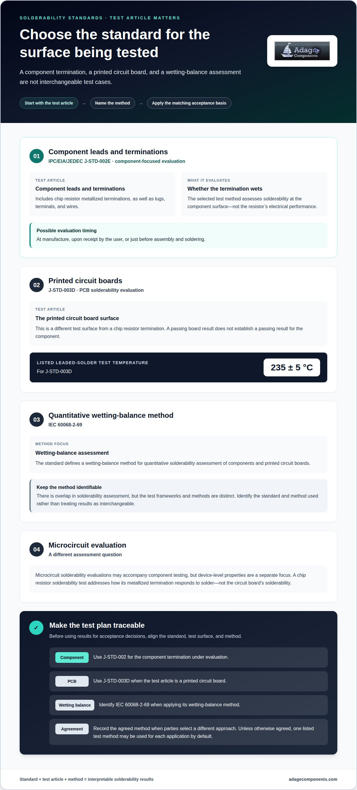
For chip resistor terminations, the relevant component-focused framework is IPC/EIA/JEDEC J-STD-002E. It is identified as the primary industry standard for evaluating solderability of component leads, terminations, lugs, terminals, and wires. Chip resistors have terminations rather than conventional wire leads, so the component termination is the surface under evaluation. This focus separates component solderability from printed circuit board solderability and from broader microcircuit assessments.
J-STD-002 evaluates whether a component’s termination can be wetted under a selected test method. J-STD-003D addresses solderability of printed circuit boards instead. Its listed leaded-solder test temperature is 235 ± 5 °C. The distinction matters because a board surface and a resistor termination are different test articles. A passing result for one does not establish a passing result for the other.
J-STD-002’s scope is the solderability of component leads and terminations, including chip resistor terminations; it also names lugs, terminals, and wires. The evaluation may take place at manufacture, upon receipt by the user, or just before assembly and soldering. Unless the parties agree otherwise, one listed test method may be used for each application by default. These provisions make the test choice and timing part of the agreed quality plan.
IEC 60068-2-69 defines a wetting-balance method for quantitative solderability assessment of components and printed circuit boards. That creates an area of overlap with J-STD-002: both frameworks can address component solderability through wetting behavior. The practical distinction is that J-STD-002 provides component-focused test methods and criteria, while IEC 60068-2-69 defines the wetting-balance method. A test report should identify the standard and method used, rather than treating results as interchangeable.
Microcircuit solderability evaluations may accompany component testing, but they address a different question when focused on device-level properties. A chip resistor solderability test assesses how the metallized termination responds to solder, not the resistor’s electrical performance or the circuit board’s solderability. Keeping these boundaries clear helps prevent one test result from being used to support unrelated acceptance requirements.
For a production or receiving plan, clearly identify the test article, method, and acceptance basis:
- Use J-STD-002 for the component termination under evaluation.
- Use J-STD-003D when the test article is a printed circuit board.
- Identify IEC 60068-2-69 when applying its wetting-balance method.
- Record the agreed method when parties select a different approach.
These distinctions make comparisons meaningful. Before using results to guide acceptance decisions, ensure the standard, test surface, and method align.
The revision identified is IPC/EIA/JEDEC J-STD-002E. It evaluates solderability at the component termination, including chip resistor terminations, and distinguishes that assessment from printed circuit board solderability.
Component preconditioning and accelerated aging
Preconditioning exposes a component to controlled environmental stress before solderability testing. Under IPC J-STD-002D, the default condition is a dry bake at 155 °C for 4 hours, with a tolerance of 15 minutes. This step helps assess termination wetting after simulated storage or handling, rather than testing only freshly prepared parts.
J-STD-002 distinguishes surface-mount chip resistor testing by treating the metallized terminations as the test surfaces. The applicable method accounts for the component’s form and termination geometry, unlike tests designed around leads. That distinction affects sample positioning, exposure, and how results are judged.
The current revision identified for J-STD-002 is revision E. Revision selection matters because the test procedure and acceptance basis must correspond to the edition named in the quality agreement; the available facts do not identify a specific revision E change affecting chip components.
Dry-heat baking and steam aging create different pretest conditions. Dry baking applies heat without the moisture exposure used in steam aging. For optional legacy testing of all finishes, J-STD-002D lists a 4-hour preconditioning duration with a 10-minute tolerance. Keep that legacy condition distinct from the default dry-bake condition, which has a 15-minute tolerance.
Steam aging stresses terminations with heat and moisture. For locations at elevations of 0-305 m, J-STD-002D specifies a steam temperature of 93 ± 3 °C. The described steam-aging condition uses 100% relative humidity; a separate dip-and-look example uses 8 hours at 93°C with 98% RH. These conditions should not be treated as interchangeable: the test plan must identify which exposure applies.
For wetting-balance testing, steam aging may continue for up to 8 hours. Accelerated aging is described as simulating approximately 6 to 12 months of storage before solderability evaluation. This provides a way to assess whether stored components retain solderable terminations, but it does not replace controlled storage or define every product’s shelf-life.
Preconditioning records should capture the chosen exposure and its tolerance alongside the test method. For example, a report can distinguish a 155 °C dry bake from steam aging at 93 ± 3 °C, then link the exposure to the solderability result. This traceability helps explain whether a failure reflects the termination condition after aging or a different test setup.
Dip-and-look test procedure and acceptance criteria
The IPC J-STD-002 solderability test protocols for chip resistors evaluate termination wetting using a defined method and acceptance area. Dip-and-look provides a visual assessment after controlled exposure to molten solder.
Dip-and-Look Test Steps
The dip-and-look test exposes a prepared sample to molten solder, then inspects the termination for wetting. In one procedure example, the sample enters the bath at 25 mm/s and remains immersed for 3 to 5 seconds. An SnPb example uses a bath at 245°C ± 5°C. These settings illustrate a test procedure, not interchangeable conditions for every method.
J-STD-002 identifies Test B for leadless components using SnPb solder. Lead-free Test B1 specifies a 5-second immersion, with a +0/−0.5-second tolerance. The selected method and alloy establish the conditions for evaluating the termination’s response.
Visual Solder Coverage
Visual coverage is the portion of the defined termination area covered continuously by solder after immersion. IPC J-STD-002 generally requires at least 95% continuous coverage on each termination’s critical area, while exposed pads generally require at least 80%.
Inspection looks for continuous, smooth, bright coverage, not simply isolated solder deposits. The IPC J-STD-002 solderability test protocols for chip resistors use a stated criterion of 95% coverage on the tested surface. Inspection at 10x to 20x magnification helps distinguish continuous wetting from bare areas or visible discontinuities.
Results and Reporting Requirements
Acceptance is assessed against the applicable method and area. A wetting angle below 90 degrees indicates acceptable wetting. Reports should identify the criterion used and the inspected surface, since exposed pads and termination critical areas have different general coverage thresholds.
Record the test method, alloy, bath conditions, immersion settings, and observed coverage. For example, identifying Test B1 and its lead-free alloy prevents confusion with Test B. Reporting these details alongside the pass or fail result gives quality teams a traceable basis for reviewing chip resistor termination performance.
For engineers applying the IPC J-STD-002 solderability test protocols for chip resistors, keeping method conditions and observations together makes results easier to interpret across evaluations.
Consistent preparation and inspection help tie visual judgments to the selected procedure. Ensure the full relevant termination area is visible, and assess whether solder coverage is continuous rather than present only in isolated spots. If a result is unclear, record the observation as uncertain and review it against the selected acceptance criterion. A bright deposit alone does not prove adequate wetting. Recording observation notes alongside the method conditions helps reviewers understand what was assessed. This keeps the visual assessment focused on the defined surface and criterion, while highlighting appearances that need closer review.
EIA/IPC/JEDEC J-STD-002D includes a solder bath/dip-and-look test for leadless components using SnPb solder, designated Test B. The dip-and-look inspection is performed under 10× to 40× magnification. Notes should distinguish visible continuity from areas where the observation is uncertain. Such documentation preserves the basis for a later review without replacing the acceptance criterion selected for the test.
Flux application and solder-bath conditions
Flux, alloy, bath temperature, and immersion settings form one controlled test setup. Their values depend on the J-STD-002 method selected for the chip resistor termination.
There is no single bath temperature, alloy, immersion time, or depth for every method. For lead-free Test B1, the listed SAC solder condition is 245 ± 5 °C, with 5 seconds immersion and a +0/−0.5-second tolerance. A wetting-balance globule test lists 1 mm immersion depth and 2.5 seconds for a 0603 (0201) resistor size.
A separate dip-and-look procedure example uses an SnPb bath at 245°C ± 5°C. It immerses the sample at 25 mm/s for 3 to 5 seconds. Treat these as method-specific conditions, not values to combine into one procedure. The test method determines the applicable alloy and settings.
Flux application also follows the selected procedure. The described dip-and-look process applies the sample to low-activity rosin flux for 5 to 10 seconds. J-STD-002D specifies Flux #1 as containing 0.15 ± 0.01 weight parts of diethylammonium hydrochloride, with maximum chlorine content of 0.2% of solids. Flux identity and exposure should be recorded with the bath conditions.
Bath composition is another controlled variable. J-STD-002D gives a maximum copper contaminant limit of 0.300 for SnPb solder alloys. For lead-free solder alloys, it lists maximum limits of 4.000 for silver contaminants and 0.100 for lead contaminants. These limits make alloy condition part of test control, not just a material choice.
A workable setup includes a solder bath, the alloy and flux specified by the method, a sample holder or immersion mechanism, temperature measurement, and visual inspection equipment. Check or calibrate temperature measurement and immersion controls under the laboratory’s quality process. This supports repeatable settings but does not replace the values prescribed by the method.
Before testing, document the method, alloy, flux, bath temperature, immersion rate, time, and depth where the method specifies one. For example, a Test B1 record should distinguish its SAC condition and 5-second immersion from the SnPb dip-and-look example. This prevents a result from being interpreted against conditions intended for another method.
For chip resistor evaluations, consistency across the complete setup is a practical control point. Changes in flux exposure, bath contamination, or immersion settings can affect wetting observations. Record each variable alongside the result to give quality teams a traceable basis for comparing samples and reviewing solderability acceptance.
Lead and lead-free solder alloys and test temperatures
J-STD-002 distinguishes solderability tests by alloy and method, so a temperature cannot be separated from its test designation. SnPb and lead-free conditions use different alloy controls, and the selected procedure determines which values apply. For chip resistor terminations, record the alloy and method together to keep test results interpretable.
For lead-free Test B1, IPC J-STD-002D lists SAC solder at 245 ± 5 °C, with a 5-second immersion and a +0/−0.5-second tolerance. A separate listed solder-bath test temperature for lead-free solder under J-STD-002 is 255 ± 5 °C. These are distinct conditions, not interchangeable settings. The test designation identifies the applicable procedure.
SnPb solder appears in component solderability methods as well. J-STD-002D identifies Test B as a solder bath and dip-and-look method for leadless components using SnPb solder. A separate SnPb surface-mount process simulation is designated Test S. Test D addresses resistance to dissolution or dewetting of metallization and applies to both SnPb and lead-free solder. Each method evaluates a different response, so alloy selection should follow the test objective.
Process-simulation reflow also uses alloy-specific thermal profiles. IR/convection simulation uses a controlled reflow profile, distinct from bath-test settings. Its preheat range is 150-180 °C for 60-120 seconds. Vapor-phase lead-free reflow uses 217-240 °C with a dwell of 45-90 seconds. These profiles simulate assembly exposure; they are not bath-test settings.
For lead-free oven reflow, J-STD-002D lists 230-250 °C for 2-5 minutes, until reflow is assured. Comparing this with the IR/convection and vapor-phase profiles shows why a report must name the heating method. Similar peak ranges do not make dwell times or process conditions equivalent.
In practice, a test plan should specify the solder alloy, method, temperature, and exposure time as a single condition set. For example, identify Test B1 when applying its SAC bath condition, rather than labeling a result only “lead-free.” This prevents a Test B1 bath result from being confused with a surface-mount reflow simulation or an SnPb Test B evaluation.
Use the applicable procedure to select the alloy and thermal profile, then preserve those details in the test record. To review resistor categories for component planning, explore the resistor linecard.
Adage Components: Thick Film Chip Resistors
Adage Components supplies Thick Film Chip Resistors for procurement teams aligning component selection with assembly requirements. We work with vetted manufacturers and partner suppliers, many franchised by top 100 distributors, to support authentic component sourcing. Our support includes commercial and automotive grade components and compliance with all ISO certifications.
As a private-label manufacturer, Adage Components also offers Thin Film Precision Resistors and Carbon Film Resistors at one of the best costs in the industry. Customers get manufacturer pricing and OEM pricing, with the same advantages as buying from tier 1 distributors but at OEM pricing. Our amazing international logistic program and growing state-of-the-art warehouse support short lead times, fit with your MRP system, and delivery to your facility in real time, on time.
If you’re planning a resistor purchase or reviewing sourcing options, contact Adage Components to discuss your component needs.
Put Your Solderability Criteria to Work
Turn your test expectations into clear purchasing and quality requirements. Use the IPC J-STD-002 solderability test protocols for chip resistors to align engineering, quality, and procurement on the evaluation basis before components enter an assembly workflow. A shared specification gives teams a practical reference for reviewing supplier documentation and resolving differences in acceptance expectations.
Make the next step a focused sourcing review. Define the resistor category, application requirements, and documentation your team needs, then keep those requirements connected to your component selection process. This helps procurement decisions support the technical criteria established by your quality team without treating a solderability result as a substitute for broader component qualification.
Explore resistor options with Adage Components to support your sourcing plans. With clear requirements in place, your team can move forward with greater confidence and a more coordinated evaluation process.
Frequently Asked Questions
What solderability test methods in J-STD-002 apply to chip resistors?
Dip-and-look and wetting-balance methods can evaluate chip resistor termination wetting, while process-simulation methods assess solderability under assembly-like exposure. J-STD-002D identifies Test B for leadless components using SnPb solder, Test B1 for lead-free solder, and Test S for surface-mount process simulation. Test D addresses resistance to metallization dissolution or dewetting. Select the method that matches the evaluation objective and documented acceptance basis.
What specimen preparation and conditioning are required for chip resistor solderability tests?
Preparation depends on the selected method and agreed test plan. Keep samples identified by lot and finish so results can be traced to the evaluated components. A typical recommended storage-temperature range for components and PCBs is 15-30°C. The protocol may call for dry-bake or steam preconditioning; record the exposure used and keep it distinct from storage conditions. Avoid combining results from samples with different preparation histories.
What wetting and coverage criteria determine whether chip resistor terminations pass?
Assess the termination against the method’s defined acceptance area, not an overall visual impression. The general criterion is at least 95% continuous coverage on the critical area, while exposed pads generally use at least 80%. A wetting angle below 90 degrees indicates acceptable wetting. For consistent review, report which termination area was assessed and distinguish bare regions from discontinuities within the wetted surface.
What are common failure modes, risks, and troubleshooting steps for chip resistor solderability testing?
Common observations include incomplete wetting, dewetting, and insufficient continuous coverage. First compare the result with the chosen method’s alloy, flux, bath condition, and immersion settings; a setup mismatch can make the finding difficult to interpret. For wetting-balance globule testing, the criterion is at least 50% of maximum theoretical force at or before 2 seconds. Test D separately addresses metallization dissolution or dewetting resistance.
Which IPC J-STD-002 revision is current, and what changes affect chip components?
Revision E is current. Chip resistors are evaluated at their metallized terminations, but no specific change in Revision E affecting chip components is identified.
Disclaimer
Cross-referenced components needs to be confirmed by the client with either spec. sheet or samples or both.
Please note, we use AI to help us, information is verified to be correct but we can not guarantee 100% accuracy.


