

What if the passive component isn’t the cause of the bridge? When avoiding passive component solder bridging on ultra-fine pitch boards, the defect often points to an interface problem involving the PCB land pattern, solder paste, placement accuracy, or reflow profile. Changing the part before checking those variables can add cost without addressing the root cause.
Repeated bridges mean rework, yield loss, and schedule pressure. Because several process variables can produce similar defects, a controlled investigation is more reliable than changing design or assembly settings by guesswork. This article explains how to identify likely contributors, check the component-to-board interface, and troubleshoot in a disciplined sequence.
Component sourcing can be part of that assessment, but it shouldn’t be mistaken for a process cure. Adage Components supplies private-label electronic components, including resistors, capacitors, and diodes, and supports OEMs and EMS providers with technical support, manufacturing audits, and international logistics. The goal is to separate evidence about the part from evidence about the assembly process.
Key Takeaways
- Map bridge locations, component references, board positions, and production lots to identify patterns before changing the process.
- For avoiding passive component solder bridging on ultra-fine pitch boards, investigate the full interface: PCB lands, solder paste, placement, and reflow.
- Compare inspection findings with process records, then isolate variables and validate one controlled change at a time.
- Use component and PCB documentation to check package, termination, footprint, and assembly compatibility.
- Use component traceability to support lot-level investigations, while keeping sourcing quality distinct from assembly-process controls.
What solder bridging looks like on ultra-fine-pitch boards, and why passive parts get blamed
A solder bridge is an unintended connection of solder between conductive features that are designed to remain electrically separate. On a populated board, it may appear as a continuous solder path joining adjacent component terminations, PCB pads, or another nearby conductive area. The key evidence is the connection itself, not simply a shiny, uneven, or oversized solder deposit.
That distinction matters during inspection. Solder extending beyond a termination may look concerning, but if it doesn’t connect to a neighboring conductive feature, it isn’t a bridge. Record it as a separate observation and assess it against the assembly’s applicable acceptance criteria. Accurate classification helps prevent teams from mixing different defect signatures and changing the process for the wrong reason.
Where bridging appears around chip resistors and other passives
Chip resistors and other surface-mount passives sit close to conductive features, so a bridge may form between their opposing terminations, between neighboring pads, or from a pad to another nearby exposed feature. A thick film chip resistor can be where the defect is visible without being the source of excess or misplaced solder.
As board density increases and spacing narrows, the available process margin decreases. Paste volume, print registration, placement accuracy, pad geometry, and reflow behavior have less room for variation before solder reaches a feature it should not join. Solder mask also separates exposed conductive areas. The solder mask can help limit solder spread, but its layout and condition are only part of the board-level picture.
Why a bridge does not automatically mean the component is at fault
A component’s body dimensions and termination geometry affect how it aligns with the footprint and how solder wets its terminations. Those details deserve inspection, especially if defects repeatedly occur on one package or lot. But a sound part can still bridge if the stencil transfers excess paste, the print is misregistered, the pads are poorly matched to the package, or placement shifts paste-to-pad alignment.
These factors can compound. A small placement offset may matter more when paste is already deposited near the edge of a pad; reflow can then draw solder into an adjacent gap. Board registration and local layout can also make the same print or placement variation produce different results across a panel. That is why avoiding passive component solder bridging on ultra-fine pitch boards starts with distinguishing where the bridge formed from what may have contributed to it.
Build the diagnosis from evidence: examine the board and bridge location, compare affected and unaffected areas, review print, placement, and reflow records, and inspect the component’s geometry and terminations. A component change is justified only when findings point to a component-related issue. Without that evidence, replacing the part risks leaving the actual process or footprint cause untouched.
How solder bridging forms: the component, paste, placement, and reflow interface
A bridge can begin before a component reaches the board. If paste deposits spread beyond their intended pads or land too close to neighboring features, they may connect during printing or merge as solder melts in reflow. Misalignment between the stencil, PCB, and component can further narrow the gap between deposits. The finished defect reflects this interface, not necessarily a single faulty input.
Several small deviations in paste transfer, board registration, placement, and reflow can combine to create a solder bridge even when no single variable appears far out of control. That’s why avoiding passive component solder bridging on ultra-fine pitch boards requires checking evidence at each process step before changing settings.
Solder-paste printing, stencil aperture, and board alignment
Start with the print. Compare solder paste inspection data for affected and unaffected boards, focusing on deposit volume, area, height, and position relative to the pads. A deposit can be within an overall volume target yet still be misplaced toward a neighboring feature. Review the stencil for contamination, wear, damage, or blocked apertures, and check whether its aperture design matches the board’s land pattern and the assembly’s documented requirements.
Then map defects across the panel. Bridges that recur in a similar position on multiple boards may point to a repeatable registration or print-transfer pattern. Defects scattered across the panel suggest a different pattern and warrant a broader review. Compare panel coordinates with inspection data, stencil alignment records, and PCB fiducials. This can help distinguish a localized offset from a deposit issue affecting the same footprint everywhere.
Use measured print data to guide any stencil change. Reducing an aperture or changing its shape without confirming what the current process deposits can shift the problem, create insufficient solder, or obscure the underlying alignment issue. Document the proposed change and assess it against the applicable board and assembly requirements.
Component placement and reflow conditions
Placement determines whether component terminations sit over their intended paste deposits. Review machine records for placement offset and rotation, and inspect whether parts are seated consistently. A small offset can leave one termination poorly aligned with its pad while pushing solder closer to an adjacent feature. Compare placement data from bridged and unaffected locations, including their positions on the board and panel.
Reflow is another variable to investigate, not an automatic culprit. Review the recorded profile against the approved process window and the requirements for the materials and components in use. Consider whether bridge locations align with any profile or production change, but don’t assume temperature or conveyor speed caused the defect based on appearance alone. Validate any adjustment on the specific assembly before applying it to production.
Keep the component reference and footprint aligned with the documentation used for the build. Adage Components’ passive component line card can support component identification during that review. Change one controlled variable at a time, preserve the baseline records, and compare the resulting inspection data so the effect is traceable.
How to diagnose the root cause before changing components or process settings
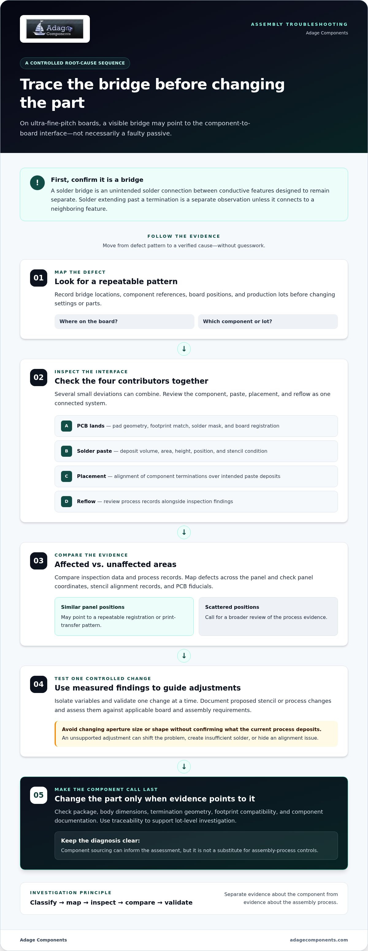
A repeatable investigation separates a defect’s location from its cause. Before changing a component, stencil, placement program, or reflow setting, capture enough detail to compare bridged boards with unaffected boards from the same build. This evidence helps reveal whether the pattern follows a board position, process condition, component reference, or production lot.
- Map each defect. Record the board location, bridge orientation, component reference, panel position, and production lot. Photograph representative examples and link each image to its inspection record. Consistent labels make patterns easier to compare across boards and builds.
- Inspect the physical evidence. Examine the bridge and nearby pads, component terminations, paste residue, and any visible component damage. Use optical or other inspection methods suited to the feature and production plan. Record observations before cleaning or rework changes the evidence.
- Compare process records. Review paste inspection, placement, and reflow data for affected and unaffected boards. Match records to board and panel coordinates where possible. Look for a shared print-position offset, placement condition, or process change, rather than relying on a single defective sample.
- Isolate a variable. Use the defect pattern to prioritize a test, then change one process variable at a time. Keep other conditions stable and document the baseline, adjustment, and result. Avoid changing the component and process settings together, since that makes the outcome difficult to interpret.
- Validate the change. Inspect boards produced under the controlled trial and compare the findings with the original defect map. Confirm that the bridge pattern changes as expected without introducing a different defect. Record the validated condition in the applicable production documentation.
Build a defect map and inspect the physical evidence
Use clear, repeatable identifiers: board and panel coordinates, component designator, bridge orientation, lot, and inspection image. Check whether solder joins adjacent pads or terminations, and note nearby deposits, residue, or damage without assuming they caused the connection. Apply inspection methods and acceptance criteria defined by the production plan; don’t infer defect severity from appearance alone.
Use pattern analysis to prioritize likely causes
Ask whether defects cluster by board location, component type, machine, or lot. A recurring panel position may direct attention to print or registration data; a pattern limited to one component reference or lot warrants closer comparison of part geometry and condition. These patterns guide the next check, but don’t prove a cause on their own.
Change one controlled variable at a time, and document the result. If evidence consistently follows a component lot across board positions while process records remain comparable, escalate the lot-level investigation. If defects track a machine or panel location instead, investigate that process or position first. This evidence-led sequence supports avoiding passive component solder bridging on ultra-fine pitch boards without treating correlation as proof.
How to prevent solder bridges with a controlled design and assembly plan
Prevention works best as a linked set of controls, not a single stencil or reflow adjustment. Design documentation should match the component and PCB; production checks should then confirm that paste printing, placement, and reflow stay within the approved process. Inspection closes the loop by showing whether a corrective action changed the defect pattern without creating another assembly issue.
Reduce design and component-interface risk
Review the PCB footprint and pad geometry against the applicable component documentation. Confirm the package identity, termination configuration, and visible condition when investigating a part-related pattern. For substitutions, document the approved component and verify that its footprint and assembly process remain compatible. This gives engineering and production teams a common reference before a design or sourcing change reaches the line.
Control the assembly process and confirm corrective actions
Use documented checks for print quality, placement accuracy, reflow records, and post-process inspection. Set each check against the actual board, component documentation, and approved production plan. Avoid universal settings: a change suitable for one footprint or assembly may not transfer to another. Compare inspection results before and after each controlled correction to confirm that the recurring bridge pattern has been reduced.
- Design review: Check land patterns, pad geometry, solder-mask definition, and component documentation together before releasing a board revision.
- Print control: Monitor deposit position and consistency, and inspect stencil condition when the evidence points to a printing issue.
- Placement verification: Compare machine records and component seating with the intended pad and paste alignment.
- Reflow monitoring: Review recorded profiles against the approved process window; validate adjustments for the specific assembly.
- Inspection: Track bridge location and pattern across subsequent production, using the criteria in the production plan.
Keep the before-and-after records tied to the board revision, component identification, production lot, and process change. If the defect persists, return to the evidence and reassess the suspected contributor rather than layering on additional adjustments. For avoiding passive component solder bridging on ultra-fine pitch boards, this traceable feedback loop helps teams distinguish a lasting corrective action from a temporary improvement.
Align component selection with the assembly plan by reviewing Adage Components’ passive component line card as part of your design and sourcing workflow.
When component sourcing belongs in the solder-bridge prevention plan
Review sourcing when defect evidence points to a repeatable component-related pattern, such as a bridge that follows a part lot across different board positions and assembly runs. Procurement records can help engineering identify the material used and compare it with the approved design basis. This investigation supports traceability, but it doesn’t replace checks of the PCB, print, placement, or reflow process.
Distinguish a component issue from a process issue
Compare defect patterns across component lots, board locations, and production runs. If a pattern appears to follow one lot, review its identification and available documentation alongside assembly records. If it instead clusters by panel position or production run, focus on the related process evidence. Keep conclusions proportional to the findings: correlation can guide the next check, but it doesn’t establish that a component caused the bridge.
Connect component quality with production continuity
Reliable component identification helps teams maintain consistent procurement records and plan material requirements. Adage Components provides private-label electronic components and cost-effective alternatives for OEMs and EMS providers. These sourcing options can support procurement decisions while engineering teams continue to validate assembly controls independently.
Keep sourcing decisions connected to production needs, and use component documentation and traceability to support investigations. Explore the passive component line card to identify components for your requirements.
Turn defect investigations into stronger production controls
Make each investigation useful beyond the immediate repair. Carry validated findings into design reviews, supplier records, and production documentation so teams can recognize recurring patterns earlier and keep corrective actions consistent across future builds. This disciplined feedback loop makes avoiding passive component solder bridging on ultra-fine pitch boards part of ongoing process control, not a one-time response to a defect.
Component sourcing can support that work when traceable documentation and technical context are available. Adage Components provides manufacturing audits and technical support to help customers strengthen quality and sourcing decisions. These services complement, but don’t replace, the assembly team’s responsibility to validate board-specific process changes.
For your next production review, align component requirements with the evidence your engineering and procurement teams use to manage quality and continuity. Explore passive components for your production requirements and take the next step toward a more controlled supply plan.
Frequently Asked Questions
Can passive components themselves cause solder bridging on a PCB?
Yes, a component can contribute if its package or termination condition differs from what the footprint and process expect, but proximity alone doesn’t prove the part caused the bridge. For example, a substituted package may not align with the existing pads as intended. Compare the installed part with its approved identification and documentation, then check whether the same issue follows that component across different board positions before assigning cause.
Is a solder bridge always visible during a standard visual inspection?
No. Small bridges can be difficult to distinguish from excess solder, especially around closely spaced features or where a component body limits the viewing angle. If visual inspection is inconclusive, use an appropriate magnified or automated inspection method under the production plan. Where electrical separation is in question, apply the documented test method for the assembly. Record the inspection method so later reviews compare like with like.
What should engineers record when solder bridges appear repeatedly?
Capture enough detail to connect each defect to its production context: board revision, component reference, bridge location and orientation, panel position, production lot, date or run identification, and inspection result. Add a clear image when practical and note whether the board was inspected before or after rework. This record lets the team distinguish a recurring physical location from a pattern tied to a particular build or material lot.
Can rework remove a solder bridge without damaging nearby components?
It can, but damage is possible if the repair applies unsuitable heat or mechanical force. The method should follow the assembly’s approved rework instructions and account for nearby components, pads, and board materials. After repair, inspect the area for lifted pads, disturbed terminations, or remaining solder, then perform the required electrical checks. Treat rework as correction of an affected board, not evidence that the recurring cause has been resolved.
Does a solder bridge mean the solder-paste stencil is incorrect?
No. A stencil issue is one possibility, but a bridge can also relate to print registration, PCB pad geometry, placement, component alignment, or reflow conditions. Before changing the stencil, compare solder-paste inspection results from bridged and unaffected locations. If deposits are consistently shifted or excessive near the same features, the evidence may support reviewing stencil condition or aperture design. Validate any adjustment on the actual assembly.
How can production teams tell a component-lot issue from a process issue?
Compare boards using different component lots under similar assembly conditions, and compare the same lot across board positions or production runs. If the defect follows one lot despite changes in board location, review part identification and lot documentation. If it clusters around a machine, panel position, or run regardless of lot, investigate the corresponding process records. These comparisons help prioritize checks, but the pattern alone doesn’t establish cause. This evidence-led approach supports avoiding passive component solder bridging on ultra-fine pitch boards.
When should a team review component documentation during a bridging investigation?
Review it when the installed part’s identity is uncertain, a substitution has occurred, or findings suggest the defect follows a particular component type or lot. Compare the part number and package information with the approved bill of materials and PCB footprint. Check available documentation for termination details and any assembly guidance relevant to the investigation. This helps determine whether the component matches the design basis before teams revise the footprint or process.
Disclaimer
Cross-referenced components needs to be confirmed by the client with either spec. sheet or samples or both.
Please note, we use AI to help us, information is verified to be correct but we can not guarantee 100% accuracy.


